- 您现在的位置:买卖IC网 > Sheet目录1253 > XR16M890IL32-0C-EB (Exar Corporation)BOARD EVAL XR16M890IL32
�� �
�
�XR16M890�
�REV.� 1.0.0�
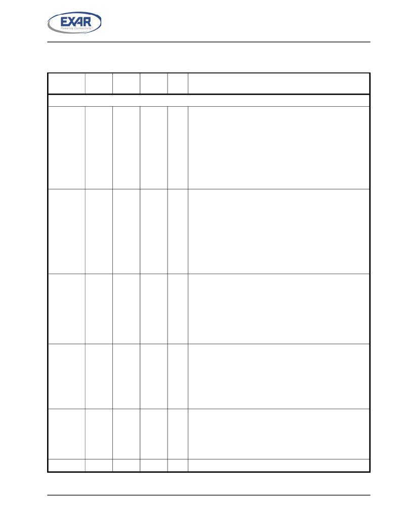
�PIN� DESCRIPTIONS�
�Pin� Description�
�UART� WITH� 128-BYTE� FIFO� AND� INTEGRATED� LEVEL� SHIFTERS�
�N� AME�
�QFN-32�
�P� IN� #�
�QFN-40� TQFP-48�
�PIN#� PIN#�
�T� YPE�
�D� ESCRIPTION�
�DATA� BUS� INTERFACE� -� Intel/Motorola�
�16/68#�
�32�
�1�
�1�
�I�
�Intel� or� Motorola� Bus� Select.� This� pin� selects� the� 16� or� 68� mode�
�when� VLIO_EN� is� a� logic� 0.� In� the� VLIO� mode� (VLIO_EN� is� a� logic�
�1),� this� pin� becomes� the� SLEEP/PWRDN#� pin� in� the� QFN-32� pack-�
�age.�
�When� 16/68#� pin� is� at� logic� 1,� 16� or� Intel� Mode,� the� device� will� oper-�
�ate� in� the� Intel� bus� type� of� interface.�
�When� 16/68#� pin� is� at� logic� 0,� 68� or� Motorola� mode,� the� device� will�
�operate� in� the� Motorola� bus� type� of� interface.� This� pin� does� not� have�
�an� internal� pull-up� or� pull-down� resistor.�
�A2�
�A1�
�A0�
�29�
�30�
�31�
�38�
�39�
�40�
�46�
�47�
�48�
�I�
�Address� lines� [2:0].� These� 3� address� lines� select� the� internal� regis-�
�ters� in� UART� channel� during� a� data� bus� transaction.�
�In� the� VLIO� bus� mode� (details� on� next� page):�
�■�
�■�
�■�
�■�
�A2� becomes� ENIR#�
�A1� becomes� ENRS485#� in� the� QFN-32� package�
�A1� is� an� unused� input� on� the� TQFP-48� and� QFN-40�
�packages� and� should� be� connected� to� GND�
�A0� becomes� LLA#�
�D7�
�D6�
�D5�
�D4�
�D3�
�D2�
�D1�
�D0�
�IOR#�
�8�
�7�
�6�
�5�
�4�
�3�
�2�
�1�
�13�
�9�
�8�
�7�
�6�
�5�
�4�
�3�
�2�
�16�
�9�
�8�
�7�
�6�
�5�
�4�
�3�
�2�
�10�
�I/O�
�I�
�Data� bus� lines� [7:0]� (bidirectional).�
�In� the� VLIO� bus� mode,� D7:D0� becomes� AD7:AD0.�
�When� 16/68#� pin� is� at� logic� 1,� the� Intel� bus� interface� is� selected� and�
�this� input� becomes� read� strobe� (active� low).� The� falling� edge� insti-�
�gates� an� internal� read� cycle� and� retrieves� the� data� byte� from� an�
�internal� register� pointed� by� the� address� lines� [A2:A0],� puts� the� data�
�byte� on� the� data� bus� to� allow� the� host� processor� to� read� it� on� the� ris-�
�ing� edge.�
�When� 16/68#� pin� is� at� logic� 0,� the� Motorola� bus� interface� is� selected�
�and� this� input� should� be� connected� to� VCC.�
�IOW#�
�14�
�17�
�11�
�I�
�When� 16/68#� pin� is� at� logic� 1,� it� selects� Intel� bus� interface� and� this�
�(R/W#)�
�input� becomes� write� strobe� (active� low).� The� falling� edge� instigates�
�the� internal� write� cycle� and� the� rising� edge� transfers� the� data� byte�
�on� the� data� bus� to� an� internal� register� pointed� by� the� address� lines.�
�When� 16/68#� pin� is� at� logic� 0,� the� Motorola� bus� interface� is� selected�
�and� this� input� becomes� read� (logic� 1)� and� write� (logic� 0)� signal.�
�CS#�
�15�
�18�
�12�
�I�
�This� input� is� chip� select� (active� low)� to� enable� the� device.�
�5�
�发布紧急采购,3分钟左右您将得到回复。
相关PDF资料
XR18W750/753-0B-EB
EVAL BOARD FOR XR18W750/753
XRP2526EVB
BOARD EVAL POWER SWITCH XRP2526
XRP2528EVB
BOARD EVAL POWER SWITCH XRP2528
XT800SM
GAS TRIGGER TUBE 800V SMD
YMCRPR8C25
REF PLATFORM MOTOR CTRL R8C/25
ZB3251
INLINE FUSE HOLDER PLASTIC BODY
ZB3260
INLINE FUSE HOLDER BAKELITE BODY
ZB3270
PANEL MOUNT FUSE HOLDER
相关代理商/技术参数
XR16M890IL32-F
功能描述:UART 接口集成电路 1-Ch 8 Bit/VLIO UART w/Lvl Shftrs & 4GPIO
RoHS:否 制造商:Texas Instruments 通道数量:2 数据速率:3 Mbps 电源电压-最大:3.6 V 电源电压-最小:2.7 V 电源电流:20 mA 最大工作温度:+ 85 C 最小工作温度:- 40 C 封装 / 箱体:LQFP-48 封装:Reel
XR16M890IL32TR
制造商:EXAR 制造商全称:EXAR 功能描述:UART WITH 128-BYTE FIFO AND INTEGRATED LEVEL SHIFTERS
XR16M890IL32TR-F
功能描述:UART 接口集成电路 1-Ch 8 Bit/VLIO UART w/Lvl Shftrs & 4GPIO
RoHS:否 制造商:Texas Instruments 通道数量:2 数据速率:3 Mbps 电源电压-最大:3.6 V 电源电压-最小:2.7 V 电源电流:20 mA 最大工作温度:+ 85 C 最小工作温度:- 40 C 封装 / 箱体:LQFP-48 封装:Reel
XR16M890IL40
制造商:EXAR 制造商全称:EXAR 功能描述:UART WITH 128-BYTE FIFO AND INTEGRATED LEVEL SHIFTERS
XR16M890IL40-0C-EB
功能描述:UART 接口集成电路 EVAL F/M890 QFN40 MOT, INTEL, VLIO INT RoHS:否 制造商:Texas Instruments 通道数量:2 数据速率:3 Mbps 电源电压-最大:3.6 V 电源电压-最小:2.7 V 电源电流:20 mA 最大工作温度:+ 85 C 最小工作温度:- 40 C 封装 / 箱体:LQFP-48 封装:Reel
XR16M890IL40-F
功能描述:UART 接口集成电路 1-Ch 8 Bit/VLIO UART w/Lvl Shftrs & 8GPIO
RoHS:否 制造商:Texas Instruments 通道数量:2 数据速率:3 Mbps 电源电压-最大:3.6 V 电源电压-最小:2.7 V 电源电流:20 mA 最大工作温度:+ 85 C 最小工作温度:- 40 C 封装 / 箱体:LQFP-48 封装:Reel
XR16M890IL40TR
制造商:EXAR 制造商全称:EXAR 功能描述:UART WITH 128-BYTE FIFO AND INTEGRATED LEVEL SHIFTERS
XR16M890IL40TR-F
功能描述:UART 接口集成电路 1-Ch 8 Bit/VLIO UART w/Lvl Shftrs & 8GPIO
RoHS:否 制造商:Texas Instruments 通道数量:2 数据速率:3 Mbps 电源电压-最大:3.6 V 电源电压-最小:2.7 V 电源电流:20 mA 最大工作温度:+ 85 C 最小工作温度:- 40 C 封装 / 箱体:LQFP-48 封装:Reel